Sumitomo Metals Develops Technology to Grow Silicon Carbide Single Crystal for Energy Saving Power Devices
2008.10.16
- Sumitomo Metal Industries, Ltd.
The Corporate Research & Development Laboratories of Sumitomo Metal Industries, Ltd. (Sumitomo Metals) has succeeded for the first time in the world in developing a solution growth method(*1) to grow silicon carbide(*2) single crystal in a high-temperature solution of metals such as silicon and titanium. This opens up the possibility of commercial use of silicon carbide energy-saving power devices(*3).
1. Background of development
Silicon carbide enables us to make small-size high-efficiency power devices, thanks to its property to withstand a higher power voltage and higher temperature than silicon. It is also one of the key materials enabling energy conservation. Through improvement in applications such as replacing silicon with silicon carbide in power devices for hybrid cars and electric vehicles (EV), significant reductions in the emission of carbon dioxide
CO2 is expected. For such commercial applications, however, it is critical to create and grow single crystal wafers of large diameter and having little crystalline defects.
The conventional technology to create single crystal silicon carbide is the sublimation recrystalization technique(*4): to sublime silicon carbide powder materials and recrystalize them on the seed crystal. By using this method, silicon carbide wafers of 4 inches in diameter have been developed. But due to the presence of many crystalline defects, application of such wafers to MOSFET(*5) and other power devices has lagged.
In 2000 Sumitomo Metals began development in this field, by leveraging on its high-temperature control techniques that have been accumulated from the steel manufacturing techniques. At this time, the Company succeeded in developing a method to create single crystal silicon carbide from a solution.
2. Details of development
With assistance of NEDO(*6), Sumitomo Metals has been developing a solution growth method to grow single crystal silicon carbide from a high-temperature solution made of metals such as silicon and titanium. We succeeded in creating silicon carbide 2 inches in diameter in 2004 and 6 inches in diameter in 2006.
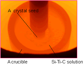
Using the solution growth method, in which crystals are grown from the solution, crystals with fewer crystalline defects than resulted when using the sublimation-recrystalization technique can be grown. We are using as the method the dipping of a crystal seed in the solution followed by pulling the seed and rotating it at the same time. Similar to the Czochralski process(*7) that is well proven for growing silicon crystal; our method should be well suited for mass production of silicon carbide.
Moreover, thanks to improvement in the accelerated rotation of seed crystal and in the crucible used, we have achieved the growth speed of over 200 μm/hr (over 1 mm in five hours), that is almost double the speed reached using the conventional technique.
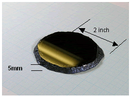
In order to commercialize the method, we need to grow crystals with a certain thickness so as to be capable of being sliced into wafers. We have improved the method and succeeded in growing single crystals 5 mm in thickness and 2 inches in diameter. We plan to grow crystals with thickness of over 10 mm within this fiscal year (ending in March 2009).
We are also using the solution growth method for growing epitaxial films(*8). We have succeeded in lowering impurity concentration in crystals by one-tenth or more compared to the conventional method. We intend to further raise the degree of purification.
3. Future developments
Sumitomo Metals will continue to improve stability in growing techniques and focus on overcoming technical challenges in order to realize early commercial application.
Graphics
(Left) Use of the solution growth method in growing silicon carbide single crystal
(Right) 2-inch silicon carbide single crystal
Technical Terms
(*1) Solution growth method: A crystalline growth method that uses precipitation behavior of crystals in supersaturated solution.
(*2) Silicon carbide (SiC): A chemical compound with superb properties: the electric field breakdown strength is about ten times more than silicon and the thermal conductivity is three times more.
(*3) Power devices: Power devices are also called power semiconductor devices. They are semiconductor devices that convert or control electric power, and are used as switches or rectifiers. Some common power devices are the power diode, thyristor, and MOSFET. They are used within the systems used in electric appliances, hybrid cars, electric vehicles, railway transport, electric power, and various industries.
(*4) Sublimation-recrystalization technique: By using the sublimation change of solid crystal materials from solid state directly to a gaseous state, with no intermediate liquid stage, this method grows crystals by cooling the sublimed gas and transitioning it once again to solid crystals.
(*5) MOSFET: The Metal-Oxide-Semiconductor Field-Effect Transistor is a device used to switch electronic signals. It is the most commonly-used field-effect transistor.
(*6) NEDO: The New Energy and Industrial Technology Development Organization is an independent administrative institution, one of the largest of its kind in Japan, and has the objective of supporting research, development, and promotion of industrial technologies as well as energy and environmental technologies.
(*7) The Czochralski process: It is a common method of crystal growth used to obtain single crystals. A seed crystal, mounted on a rod, is dipped into the melted materials in a crucible. The seed crystal's rod then is pulled upwards and rotated at the same time.
(*8) Epitaxial film: A thin film that is grown on crystal substrate and is relatively purified (has fewer defects). Epitaxy is also used to grow layers of pre-doped silicon, before they are processed into power devices