First Successful Development in Japan of Six-inch Diameter Silicon Carbide Single Crystal Wafer, by Nippon Steel
2011/12/06
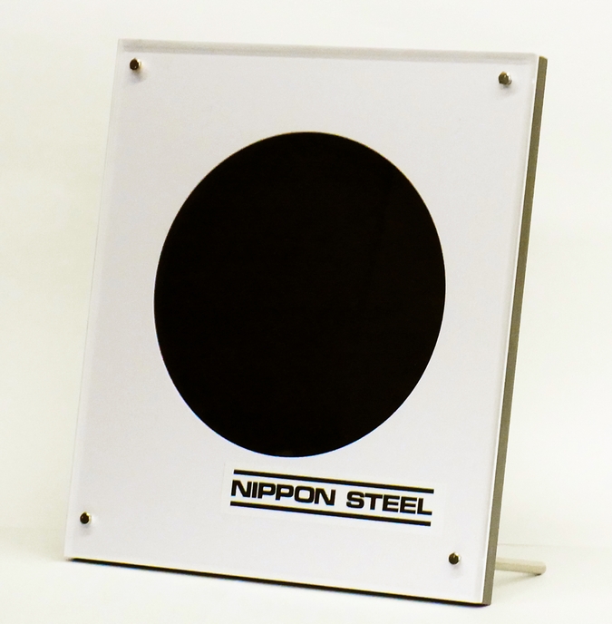
Six-inch SiC wafer to be the first in Japan
Nippon Steel Corporation (president: Shoji Muneoka) has successfully developed, at the Advanced Technology Research Laboratories of its Technical Development Bureau, six-inch diameter silicon carbide (hereinafter “SiC”) single-crystal wafer(*1), which is a key material for mass production and spread of high-performance-power semiconductor devices in the future.
1. SiC wafer, a revolutionary material for realizing low-carbon society
SiC wafer, as compared with silicon wafers being used in the manufacture of diode(*2), transistor (*3) and other semiconductor devices (*4), is capable of suppressing the power-conversion loss to less than half when used in various electronic devices. It is also excellent in both high-voltage and heat resistance properties, making it suitable for high-voltage, high-temperature uses in photovoltaic power generation, automotive (EV, HEV, etc.), and other applications of power electronics.
Broad-based spread of power semiconductors using SiC wafers, having such outstanding features, raises expectations of significant reductions in power loss in many segments and great effects in energy conservation and CO2 emission reduction.
2. Effects of 6-inch diameter SiC wafer: Cost reduction in SiC-device manufacture and expansion of application areas
High-quality SiC wafers now on the market predominantly have 3-inch and 4-inch diameters, and semiconductor-manufacturers’ development and commercialization of semiconductors are being made based upon the availability of such SiC wafers. But, there is a very strong need for greater efficiency in device production and also for the development and commercialization of SiC device in the large-current & high-voltage segment, calling for large-aperture SiC wafer to respond to these requirements.
Six-inch SiC wafer is expected to increase the efficiency of SiC device production and to decrease the cost of device manufacture.
The outcoming of 6-inch wafer will make it possible to manufacture large-area device for controlling larger current and higher voltage, thus affording to further extend applications to automobiles (EV/HEV, etc.), rapid-transit railways, and other broader areas.
Because of this great potential, 6-inch SiC wafer has also been the subject of research and development in the national project of the Ministry of Economy, Trade and Industry, as a next-generation material capable of enhancing industrial competitiveness based on energy-saving technology.
3. Development of 6-inch Diameter SiC wafer: Overcoming the problem of large diameter by the development of our own growth technologies and operating conditions of equipment.
SiC single crystal is usually manufactured by what is called the sublimation- recrystallization method. In the manufacturing equipment heated to temperatures of over 2500C, the growth of SiC single crystal is achieved by having vapor sublimated from SiC material in powder form recrystallize on top of seed crystals. In 2007, using our own sublimation- recrystallization method established through long years of R&D efforts, we pioneered in Japan in the development and establishment of the mass production technique for high-quality 4-inch wafer, then starting the sale in 2009fy by Nippon Steel Materials Co., Ltd..
In the sublimation-recrystallization method, the growth of crystals of compounds at ultra-high temperatures put difficulties in process control. The major problem was that with an increase in the size of crystal diameters, there was an increasing tendency for crystals to become susceptible to cracking induced by crystal defects(*7) and thermal stress.
By accelerating R&D efforts to resolve these problems, and based on the numerical simulation technology, we have developed the mechanism of the ultra-high-temperature equipment and the process operating conditions, suitable for the 6-inch diameter and, by successfully restraining crystal defects and crystal cracks in the growth of large-diameter crystals, succeeded in the development and manufacture of Japan’s first 6-inch aperture wafer.
It should be added that part of this R&D program was subsidized under the “Novel Semiconductor Power Electronics Project Realizing Low Carbon Emission Society” of the New Energy and Industrial Technology Development Organization (NEDO).
From now on, for the establishment of the 6-inch wafer manufacturing technology, we are going to continue efforts to achieve further product stability, to develop technology for productivity improvement, and to pursue the development of the 6-inch SiC epitaxial film(*8) manufacturing technology. The aim is to realize the marketing of 6-inch SiC single crystal wafer products, manufactures and sold by Nippon Steel Materials, and help realize the full-scale spread of SiC devices throughout the world.
For inquiries, please contact:
Public Relations Center, General Administration Div.
Tel: +81-3-6867-2135 (Mr. Suzuki)
Advanced Technology Research Laboratories, Technical Development Bureau
Tel: +81-439-80-2679 (Mr. Yano)
Tel: +81-439-80-3180 (Mr. Fujimoto)